Troubleshooting with SEM

June 29, 2022
June 29, 2022
Our eyes are useful for many tasks. They can see a bright blue finish on parts fresh out of the passivate, a smooth, satin finish coming out of a nickel tank, or those obnoxious specks of mystery material adhered to an otherwise pristine work. Unfortunately leaving it at “mystery material” is rarely good enough for the customer dealing with a pervasive staining issue.
Here’s where SEM (Scanning Electron Microscopy) comes in to save the day. While conventional microscopy can give a closer look, SEM combined with EDS (energy dispersive X-ray spectroscopy) can identify the elemental composition of even micron-sized defects.
To illustrate the benefits of SEM, here are a few examples of troubleshooting issues that would be nearly impossible or exceedingly expensive with alternative methods.
Failure Analysis 1
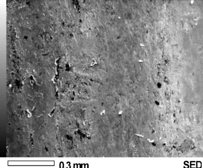
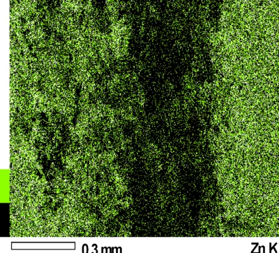
The images on the right are micrographs of the surface of a part with thin black stains across the part. The first image is a 100x magnification through that could be easily seen through other means, but the second two are unique to electron microscopy.
These are EDS images scanning for Fe and Zn selectively. The bright white and green portion of the image indicates a high concentration of the element in question.
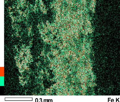
By looking at both the Fe and Zn micrographs together, we can see that the stained area has a lower concentration of Zn and a higher concentration of Fe.
In this case, since the substrate is steel, we know that the black stains are areas where the Zn did not plate well over the substrate leaving exposed Fe to be converted to oxides of Fe that appear black by the naked eye.
Failure Analysis 2
In this project, the customer had rejected parts that had pits on the surface of nickel-chrome plating. The pits were barely noticeable by the eye but could easily be felt by touch.
A microscopic image of the surface tells us almost nothing, since from the top down the defect is invisible. After cross sectioning the part, we get more detail, but with only an optical microscope, we would only see that there are 1-2 micron deep pits in the surface. But where do these pits originate?
Thanks to the distinguishing ability of SEM, we can easily see from the micrographs on the left the nickel layer and the steel substrate in each image.
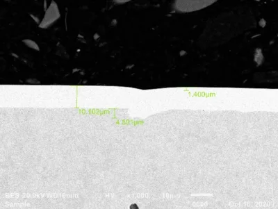
The steel is the darker gray section and the nickel above it. The third black area is the material used to mount the sample and the chrome layer is too thin at 1000x to be seen on the image. The images show us that there are pits in the substrate that are between 4 and 6 microns in depth and nearly everywhere we see these substrate pits, there is a corresponding surface pit.
Because of SEM’s contrasting of different elements in the image we can easily tell this is a substrate issue. We even know by measuring the resulting surface pit that the nickel levels the surface by about 3-4 microns.
These examples display the explanatory power of SEM analysis in the surface finishing world. The high magnification of up to 10000x allows high quality imaging of what would be impossible to see with an optical microscope.
The element contrast and elemental mapping with EDS make distinguishing between plating and substrate or plating and corrosion a simple task. For many failure analysis applications SEM is the best tool for the job, and luckily for our customers, Pavco has it.
Happy plating!
Tyler Batchler Research Chemist / SEM Technician
- Share:
-
![Facebook]()
-
![Twitter]()
-
![Mail]()
Related Articles


IT’S HOW YOU FINISH

We’re a developer and supplier of chemistries for the metal finishing industry since 1948.
In PAVCO, we develop products and deliver services of the highest quality at a reasonable cost.